Software for Windows
Science with your Sound Card!
Features:
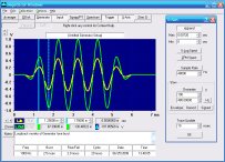
Oscilloscope
Spectrum Analyzer
8-Channel
Signal Generator
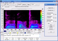
Spectrogram
Pitch Tracker
Pitch-to-MIDI
DaqMusiq Generator
(Free Music... Forever!)
Engine Simulator
LCR Meter
Remote Operation
DC Measurements
True RMS Voltmeter
Sound Level Meter
Frequency Counter
Period
Event
Spectral Event
Temperature
Pressure
MHz Frequencies
Data Logger
Waveform Averager
Histogram
Post-Stimulus Time
Histogram (PSTH)
THD Meter
IMD Meter
Precision Phase Meter
Pulse Meter
Macro System
Multi-Trace Arrays
Trigger Controls
Auto-Calibration
Spectral Peak Track
Spectrum Limit Testing
Direct-to-Disk Recording
Accessibility
Data Logger
Waveform Averager
Histogram
Post-Stimulus Time
Histogram (PSTH)
THD Meter
IMD Meter
Precision Phase Meter
Pulse Meter
Macro System
Multi-Trace Arrays
Trigger Controls
Auto-Calibration
Spectral Peak Track
Spectrum Limit Testing
Direct-to-Disk Recording
Accessibility
Applications:
Frequency response
Distortion measurement
Speech and music
Microphone calibration
Loudspeaker test
Auditory phenomena
Musical instrument tuning
Animal sound
Evoked potentials
Rotating machinery
Automotive
Product test
Contact us about
your application!
Drawing Resist Lines
The actual circuit lines can now be drawn directly on the copper surface with a "permanent" felt-tip marker. The marker acts as a "resist" to prevent the etchant from affecting the copper beneath the lines. Make sure the marker is a permanent type, since it must withstand immersion in etchant. "Sharpie" fine point permanent markers work well. Use only BLACK... other colors, even in the same marker family, are typically not as resistant to etchant. Avoid the "extra fine tip" versions... they dry out too fast during use.
You may also want a large flat-tipped marker for ground, power, mounting, or unused areas that surround the circuit. You can use "Marks-A-Lot" permanent markers for this.
Always keep the cap on the marker when not in use, even for a few seconds. When storing, keep the tip-end down. If you start to draw and the tip seems to have dried out, make a mark on plain paper to get the flow started again.
Since you will be drawing on the copper side of the board, you must flip the layout over to use the reversed image as a guide... that's why you used tracing paper or mylar. If you used a CAD system, you can just print out a reversed version for this purpose. If you used heavier graph paper, you will need to place it over a light box to see the reversed pattern.
Since you have already drilled the holes, this is now simply a case of "connect the dots" with your marker. The reason you had to sand the edges of the holes is to prevent snagging the fiber tip of the marker and pulling out wisps of felt. Also, the little "mounds" around each hole would have prevented the marker from contacting the surrounding surface. You need a small area of copper "pad" that extends all the way around each hole to aid soldering.
As you work, try to avoid contacting the board with your bare hands. You don't want to smudge the wet lines you've just drawn, of course, but you also don't want to leave hand oils in undrawn areas that will cause the marker to skip. Try working toward yourself from the furthest edge of the board, with a sheet of blank paper setting on top the undrawn portion to shield it where you must rest your hands.
While you are drawing the lines, you will undoubtedly discover a hole that you missed marking or drilling. Relax. Just draw a little pad in the proper spot, and you can drill it later, after the board is etched. Since you will usually have plenty of other points around the location, it's easy to "eyeball" where it should be drawn relative to the rest.
If you draw a line in the wrong place, let it dry for a minute and then use an ordinary pencil eraser to remove it. Make sure the eraser is clean by first rubbing it on a piece if plain paper.
If the error is a small one in a dense area of the board, you may instead opt to scrape it off gently with a sharp blade, such as an eXacto knife. This is useful, for instance, if you accidentally let two adjacent pads touch... you can just scrape a clean path between them.
After you have drawn all the traces, go back and widen the power and ground areas, possibly with a separate marker for "fill". Typically you will have a large ground area that extends from the circuit region out to the edges of the board. You can fill this in to provide a "ground plane" for better conduction and shielding, and also to reduce etchant waste.
Consider how this ground area will interact with your mounting holes. If you will be attaching the circuit to a metal case, do you want the circuit to be grounded to that case? This is typically desired for shielding purposes... but if you don't want that here, be sure to isolate pads around the mounting holes that are large enough to clear screw heads, etc.
See also Printed Circuit Construction
- Back to Board Preparation
- Ahead to Etching
- Daqarta Help Contents
- Daqarta Help Index
- Daqarta Downloads
- Daqarta Home Page
- Donate to Daqarta
Questions? Comments? Contact us!
We respond to ALL inquiries, typically within 24 hrs.INTERSTELLAR RESEARCH:
Over 45 Years of Innovative Instrumentation
© Copyright 2007 - 2026 by Interstellar Research
All rights reserved