Software for Windows
Science with your Sound Card!
Features:
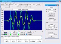
Oscilloscope
Spectrum Analyzer
8-Channel
Signal Generator
(Absolutely FREE!)
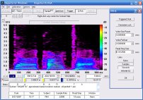
Spectrogram
Pitch Tracker
Pitch-to-MIDI
DaqMusiq Generator
(Free Music... Forever!)
Engine Simulator
LCR Meter
Remote Operation
DC Measurements
True RMS Voltmeter
Sound Level Meter
Frequency Counter
Period
Event
Spectral Event
Temperature
Pressure
MHz Frequencies
Data Logger
Waveform Averager
Histogram
Post-Stimulus Time
Histogram (PSTH)
THD Meter
IMD Meter
Precision Phase Meter
Pulse Meter
Macro System
Multi-Trace Arrays
Trigger Controls
Auto-Calibration
Spectral Peak Track
Spectrum Limit Testing
Direct-to-Disk Recording
Accessibility
Data Logger
Waveform Averager
Histogram
Post-Stimulus Time
Histogram (PSTH)
THD Meter
IMD Meter
Precision Phase Meter
Pulse Meter
Macro System
Multi-Trace Arrays
Trigger Controls
Auto-Calibration
Spectral Peak Track
Spectrum Limit Testing
Direct-to-Disk Recording
Accessibility
Applications:
Frequency response
Distortion measurement
Speech and music
Microphone calibration
Loudspeaker test
Auditory phenomena
Musical instrument tuning
Animal sound
Evoked potentials
Rotating machinery
Automotive
Product test
Contact us about
your application!
Sound Card DC Input / Output Modification
- Introduction
- Circuit Details
- Construction Details
- Calibration and Performance
- Printable Schematic and Layouts
- PCB File
Introduction:
Note: This construction project is not recommended for beginners. If you only need unipolar (positive only) DC input and/or output, see Simple Sound Card Unipolar DC Modification.
If you need bipolar input and output response at DC as well as at high frequencies, you can modify an existing sound card by adding the DC Input / Output Adapter circuit discussed here. This avoids the input AC-coupling discussed under DC Measurements And Outputs, and also allows DC or ultra-low-frequency outputs. A DC calibration voltage reference is included for convenience.
The simplest approach is to buy an inexpensive USB card, which can be combined with the DC Input / Output Adapter board housed right inside, and using the same input and output connectors.
Alternatively, you can mount the adapter board and the USB card "mother board" in an external enclosure, complete with the input and output connectors of your choice. If you only need DC inputs or DC outputs, you can implement just the parts you want. If you provide separate jacks for the DC outputs, the normal AC-coupled outputs will continue to function as before.
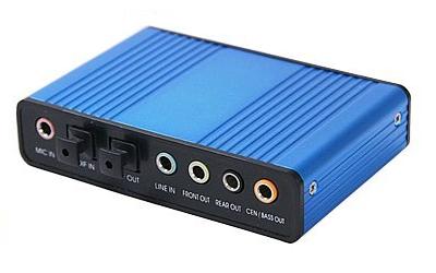
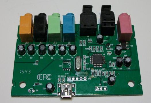
This device is readily available on the Web, with prices typically about US $25. Unfortunately, it doesn't have a specific name or model number to search for. Try "USB 5.1 Sound" and look for a matching photo. The unit shown here was purchased from HDE through Amazon.
The device uses the C-Media CM6206 USB Audio I/O Controller chip. It provides 5.1 channel output sound, which for our purposes means 6 independent and equal channels. (The so-called "Bass" or "Low Frequency" channel actually has the same full frequency response as all the others.) It has stereo Line inputs, as well as a mono Mic input which won't be used here.
Please note: If you want to use a different USB sound card for DC inputs, you must make certain that it does indeed have input circuitry... many inexpensive USB sound devices are output-only, or have only a single-channel Mic input, with no Line inputs. This appears to be true of all the small rectangular devices built onto a USB plug. Many of those also claim '5.1' or '7.1' outputs, but they have only a single stereo output jack and apparently mix the other channels to stereo internally; they don't have separately accessible output lines inside the case.
The Sound Card Performance Tests section gives information about the recommended device, plus another that uses the same CM6206 chip with 7.1 channel output. The circuit discussed here should work for that unit without changes, except that since the 7.1 device has a different board layout and component locations, the connections to it will be different.
In fact, the circuits discussed here should be generally applicable to most USB sound chipsets, even those that use a different chip than the CM6206. It's usually quite easy to locate the input and output capacitors where connections will be made, along with power and ground from the USB connector. The only tricky part may be finding where to connect to the chip's reference voltage. The "proper" way to do this is to identify the sound chip and download the product spec sheet, locate the reference pin, and trace it to some solderable location. However, some cheap USB devices don't have an identifiable chip; it may even be buried under a glob of black goo. In this case a bit of careful probing with a sharp voltmeter probe should quickly turn up an electrolytic capacitor having a DC voltage in the 1.0 to 2.5 V range. If you find two such capacitors with voltages in this range, disregard the one connected to the Mic In jack... it's a bias voltage for electret mics.
The schematic plus complete 600 DPI board and parts placement layouts suitable for printing are included in the DC_In2Out4All600.PNG file that is installed with Daqarta in the Documents - Daqarta - Circuits folder. The board supports 2 inputs and 4 outputs. It is designed to fit into the metal case by sliding into existing grooves, on the assumption that you will be using the existing input and output jacks. This makes a very neat and compact assembly.
Alternatively, you may wish to mount both the original board and the adapter in a custom case with separate connectors.
Be sure to read the Notes section of Daqarta Printed Circuits before you begin.
You can use the printed layouts directly to create your own circuit boards, with either the laser printer toner transfer method, or with the direct-draw method discussed under Printed Circuit Construction.
Alternatively, you can edit the DC_In2Out4.PCB file in the same folder to make custom modifications first. See the PCB Files discussion in Daqarta Printed Circuits for the required software to use this file, and for information on how to submit it to have boards made by a 3rd-party supplier.
Circuit Details:
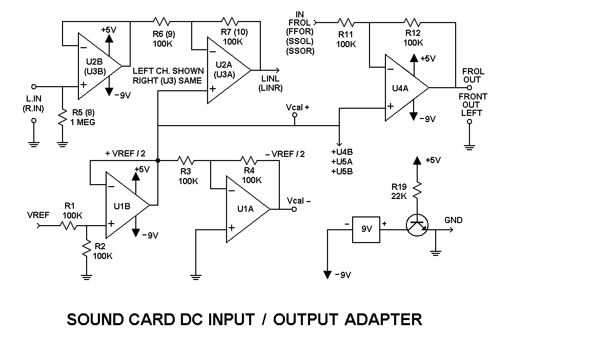
The basic problem that this circuit solves is that the input signal is bipolar, swinging above and below ground (0 V), while the internal chipset (CM6206 here) runs on a single 5 V supply and expects the signal to always be positive, swinging above and below a positive reference (typically about half the supply voltage) instead of about zero. It is thus necessary to add the reference voltage to the input signal, and connect directly to the ADC chip instead of through the AC coupling capacitors.
Likewise, the chip outputs also swing above and below that positive reference voltage, which is normally removed by AC coupling capacitors on each output line. This circuit subtracts the reference voltage directly.
The DC Input / Output Adapter uses five LF353 dual op-amps, although you can substitute other FET-input duals like TL082. It uses a 9 V "transistor radio" battery as a negative supply, and the standard +5 V USB voltage as a positive supply. A 2N3904 NPN transistor (or equivalent) acts as an automatic switch for the 9 V supply, switching on when the USB device is plugged into a USB port.
DC Input Section:
The CM6206 uses a +2.25 V reference voltage (VREF) which is provided on pin 28. Unlike some other chips, it is not buffered, so U1B provides buffering after it has been divided in half with a simple two-resistor voltage divider. This provides +1.125 V (labeled VREF/2) as a reference for all other stages, and is also the Vcal+ calibration voltage.
U1A inverts the calibration voltage to -1.125 V (Vcal-). This is only for convenience in calibration; it is not used by the rest of the circuit.
U2B provides a 1 Megohm input impedance for the signal, acting as a buffer before feeding it to the inverting input of difference amplifier U2A. Note that this doesn't look like a textbook difference amplifier circuit, which normally divides the non-inverting input in half with a pair of equal-valued resistors feeding the (+) input pin on the op-amp:
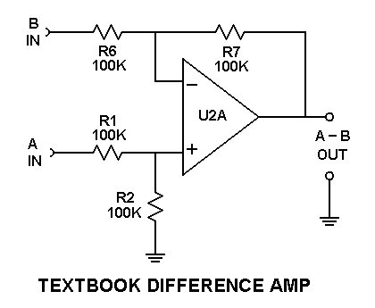
In our circuit, however, R1 and R2 are provided at the input to U1B. In both circuits, the (+) input to U2A sees VREF/2. Since that pin has an extremely high input impedance, and VREF/2 has an extremely low output impedance, the same voltage can be supplied to all 6 difference amps without interactions (2 inputs and 4 outputs).
The output of U2A (in our circuit, or the textbook form) is twice the value at its (+) pin, minus the output of U2B that feeds R6. Thus we have +2.25 V plus an inverted version of the U2B input. (You will enter a negative value into Daqarta's Full-Scale Range or External Gain controls to correct for the signal inversion during calibration.) This composite signal is then supplied directly to the chip input (LINL, pin 25), omitting the input AC coupling capacitor.
Ideally, all 100K resistors should be 1% tolerance for best results, but 5% parts should be fine for most applications. Any small gain or offset errors can be corrected in Daqarta via the External Gain and/or Zero Manual controls. (See, however, the discussion of offset error versus input range in the Calibration and Performance section below.)
DC Output Section:
The schematic shows only one of the four output channels, U4A at the upper left. U4B and both sections of U5 are identical. Each op-amp is configured as a difference circuit, exactly like the input stage discussed above, which subtracts the CM6206 chip output (IN FROL) from VREF.
Since the FROL chip output consists of the Front Out Left signal plus VREF, the U4A output is thus:
VREF - (FrontOutLeft + VREF) = -FrontOutLeft
In other words, the desired signal is inverted from what Daqarta generates, but, as for the input circuit, you can compensate for that by using a negative value in Daqarta's Full-Scale Range or External Gain controls during calibration.
The U4A section shows 'IN FROL' and 'FROL OUT' to correspond to the CM6206 pin designation for the Front Out Left channel. In parentheses below the input are 'FROR' for Front Out Right, plus 'SSOL' and 'SSOR' for Side Surround Left and Right. But since all the difference circuits are identical, the only thing that matters is that you keep track of which output is which.
Each difference circuit uses two 100K resistors, which should ideally be 1% tolerance. As for the input circuits, you can probably use 5% parts for most applications. Small gain or offset errors in Daqarta-reported values can be corrected via the External Gain and/or Zero Manual controls. In addition, the relevant Level and Offset controls for each output stream in the Generator can be used to adjust the actual output voltages.
Please note that these op-amps are not suitable for driving headphones directly. The smallest resistance that you should drive is about 1000 ohms. However, they are stable when driving normal audio cables of at least up to 12 feet (the longest tested) with 1000 ohm loads.
Construction Details:
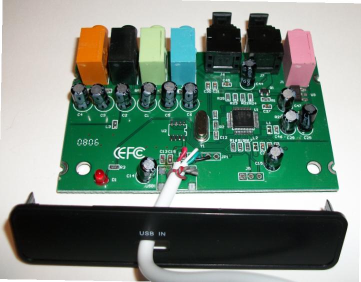
Remove the two screws that hold the rear panel onto the USB device, and push gently on the big black SPDIF TOSLINK dummy plugs to slide the circuit board and connectors out the back of the case. The board should look like this:
Note: If your board is not identical to this, you may want to download the CM6206 data sheet from the Web so you can make absolutely certain you are connecting to the proper locations. Otherwise, note that the CM6206 pins are numbered counter-clockwise, starting from the corner of the chip that has a circular depression on the top surface. On the board used for the above image, that's the upper left corner of the chip. If you use a USB device or sound card with a different chip, you will need its data sheet to find the corresponding pins.
It is strongly recommended that you not attempt to solder directly to the pins of the chip. Instead, use some other point that is connected to the given pin. For the USB device shown, there are convenient +5 and ground connections near the USB connector. The other connections can be made to the solder pads of conventional electrolytic capacitors... there is no need to solder to tiny surface mount parts, though you will need to remove the Line In surface mount capacitors and solder to their pads.
USB Socket Replacement:
While you are at it, it is also strongly recommended that you replace the mini-USB socket with a hard-wired cable. The socket is slightly too large, and the the plug sometimes loosens during use. This can cause Daqarta to hang up.
Remove the socket from the board by heating each of the four small tabs with a soldering iron while gently prying with a screwdriver inserted into the socket. After all tabs are loose the socket should easily peel off of the board at the four pin connections. Caution: Be careful not to peel back the underlying traces. It may be helpful to hold them down with an eXacto knife or some other edge while peeling the socket.
Now cut the mating plug off of the supplied USB cable. Insert the cable through the socket hole in the plastic back panel that you have previously removed. Make sure you put it through from the right direction, so you can re-install the panel later.
Carefully cut back the white (or beige) plastic cable sheath, being careful not to cut into the colored conductors. Strip about 0.25 inch from the end of each of the 4 conductors and tin with solder, then solder directly to the four tinned thru-holes in the strip marked JP1 on the board. Note that the holes may already be filled with solder on your board. If so, apply the soldering iron tip to the hole and gently push the tinned conductor end through it.
The red wire (+5 V) goes to the hole with the square pad, which is on the left-most end (as viewed with the board held so the audio jacks are at the top). Then white (DATA -), green (DATA +), and black (GROUND). See USB Cable and Connector Pinouts under Cables and Connectors in the Appendix.
The right-most hole, next to the JP1 marking, is a redundant ground connection which is handy for connecting the adapter board. Note that the adapter will also need a connection to +5 V, but you will see traces leading to other obvious connection points, including two small holes just above the +5 end.
To form a neat strain relief for the cable, loop a length of insulated solid hookup or "magnet" wire through the two holes from the bottom of the board where the USB socket was removed. Twist the ends tightly on the top so the insulated part of the cable is held firmly to the circuit board. You may want to apply a layer of hot glue as well.
Circuit Board Connections:
After fabricating the board shown in DC_In2Out4All600.PNG , either by etching your own or using the DC_In2Out4.PCB file to have it made by a 3rd-party supplier, install the components as indicated. The image below is taken from the DC_In2Out4All600.PNG and shows the parts placement in black with the bottom copper traces shown in gray:
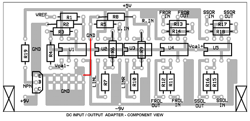
This is a single-sided board, designed for ease of home production using the direct-draw method discussed under Printed Circuit Construction. There is a single jumper on the top side, shown in red above. Resistors R6 and R9 are mounted so they straddle chips U2 and U3, respectively.
The actual board dimensions are 3.35 inches wide by 1.50 inches tall, with cutouts marked 'X' at the lower corners. The width is the same as the USB "mother" board and insures that it will slide into the grooves built into the case. This board is intended to be mounted upside down above the rear part of the USB board, and the cutouts are present to avoid interference with the rear panel mounting flanges.
Note that you should create the cutout notches before you start construction on the adapter, not after you have it stuffed with parts! If you are going to etch your own board, do this right after you have cut the board to size, before you begin any drawing or layout transfer. (A sheet metal "nibbler" tool does this easily, if you have one. Also very handy around the shop for are making equipment cases that need rectangular holes.) You don't need to cut these notches if you will be providing a separate case.
If you only want DC inputs, omit chips U4 and U5 along with resistors R11-R18. If you only want DC outputs, omit U2 and U3 and R5-R10.
Building the adapter board is moderately complex, but it is straightforward and can be done by anyone with basic soldering skills. You may think that attaching it to the USB device would be much simpler than the board construction, but unfortunately this job is complicated by the fact that the USB device uses tiny surface mount components and a multi-layer circuit board. You must use extreme caution when working on this board, to avoid damaging the circuitry.
It will be helpful to use color-coded wire to connect between the adapter board and the USB device, since there can be a lot of connections. Some of these attach to the bottom of the USB board, so be sure you leave these leads long enough to reach. If you don't have color-coded wire, you can use flaps of masking tape to temporarily label the ends that will be attached to the USB board.
Input Connections:
You'll need to remove surface mount chip capacitors C30 and C31 seen here:
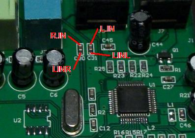
The far ends of these capacitors are connected to the Left (C31) and Right (C30) channels of the Line In jack. (Note that the Right channel is the left capacitor, and vice-versa.) Rather than trying to desolder these parts, it may be simpler to carefully crush the central portions using fine-tipped sidecutters and remove the debris, leaving the solder pad ends intact.
After removing the capacitors, wire the pads at the far ends (top of image) to L.IN and R.IN on your adapter board. The near ends go to Line In Left (LINL) and Line In Right (LINR), which are the outputs of the op-amp circuits that drive the CM6206 input pins of the same names.
Output and Reference Connections:
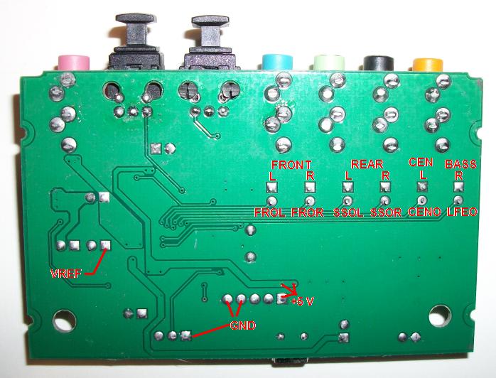
The output capacitors are the row of 6 black electrolytics near the upper left in the image under Input Connections, above. The numbering is a bit strange: Starting from the right end of the row and moving left, they are:
    C6  Front Left
    C5  Front Right
    C1  Rear Left
    C2  Rear Right
    C3  Center (Left)
    C4  Bass (Right)
These make more sense when viewed from the bottom:
If you will be providing a separate case with separate DC output connectors, you can leave these capacitors in place. That way you'll be able to get AC-coupled outputs from the existing jacks on the USB board at any time. Otherwise, to convert the existing jacks to DC outputs, you'll need to remove the coupling capacitors. (Since it can be quite difficult to desolder them, you may prefer to cut them out from the top. Use caution to avoid scraping the solder mask coating from beneath the capacitors.)
Either way, connect the round pads to the inputs of the adapter board, which in the above photo are labeled FROL (Front Out Left), FROR (Front Out Right, etc, to match the CM6206 pin names.
If you have removed the capacitors, connect the square pads to the outputs of the adapter board having the corresponding names.
If you will be using the existing connectors and installing the DC_In2Out4 board in the existing case, it will only fit if it is upside down above the rear portion of the main board. You may thus prefer to connect to the top sides of the capacitors.
The main adapter board only has 4 output circuits, so you can leave two of the 6 channels as-is, with default AC coupling. If you choose to leave the Front outputs alone, for example, then you may want to re-label the FROL and FROR connections on the adapter board to CENO and LFEO, respectively, to match the corresponding capacitor connections on the USB board.
Connect VREF from the square pad beneath capacitor C29 (as shown in the photo above) to the corresponding input on the main adapter board.
The metal case has a series of grooves on the inside. The main USB board slides into the bottom groove on each side, while the the adapter board is designed to slide into the top groove, upside down. The notches in the adapter board (marked with "X" in the component view) should be to the rear, since the rear panel mounting ears obstruct part of the grooves.
You may want to include a thin cardboard insulator sheet to prevent the solder side of the adapter from shorting out the top of the aluminum case, unless you have very neat solder connections with no protruding points.
The 9 V battery leads can be knotted as a simple strain relief and hot-glued next to the USB cable where it exits the rear of the case through the hole that used to hold the USB socket. (The battery connector can be made from the top of a discarded battery.) The battery then sits on top of the device, held in place by rubber bands around the sides of the case. The rubber also serves to reduce skidding, since there are no rubber feet on the standard case.
Note that no switch is provided for this battery since it is switched on electronically whenever the USB device is plugged into an active port. You may want to provide a switch if you expect to leave the USB device plugged in for long periods when not in use. (Note that some systems provide power to the USB ports whenever the computer is plugged in to the AC mains, even if it is in Sleep or Hibernate mode.)
Calibration and Performance:
Important: If you normally use Daqarta with a different sound card, please read the Managing Multiple Devices topic first. This discusses separate calibrations and how to select them using a separate desktop icon.
The following calibration procedures will involve changes to Full-Scale Range and External Gain in the Calibration menu. When you later exit Daqarta, you will be prompted to save calibration changes. The default filenames are Daqarta0.ATN and Daqarta0.EGN, but you should change the 0 in both of these to another numeral or letter (such as U for USB) which you will use as the N: parameter (N:U) when invoking Daqarta from the special desktop icon. (Again, see Managing Multiple Devices for details.)
The Input Line Level and Output Volume Control relative steps (dB changes) are controlled by the internal input and output attenuators and are unaffected by the DC Input / Output Adapter. If you have already performed an Auto-Calibration on this USB device, this should be OK. If not, do it now. Be sure to include the Duplex Delay option when you do this.
Input Calibration:
The useful full-scale input range is about +/-1.5 V before clipping when the Input Line Level is low (-180 or below). When the Level is maximum (0), full-scale range is about +/-40 mV.
The input frequency response, of course, now goes down to DC. The upper frequency response is unaffected, and is cut off by the CM6206 anti-alias filter above about 20 kHz.
To calibrate Full-Scale Range, you will need a DC voltage source that is about 1 V... less than a standard 1.5 V alkaline battery. (You need to be sure that the input isn't clipping, and a 1.5 V battery may be above the clip voltage.) A 1.2 V NiCd or NiMH battery will usually be OK for this use.
Fortunately, the DC Input / Output Adapter contains a built-in calibration voltage of about 1.125 V (half of the VREF voltage of 2.25 V), and additionally includes -1.125 V as well. These points are marked on the circuit board component layout as Vcal+ and Vcal-, but are not brought out to the outside of the case. So if you use these, you must perform the calibration with the rear panel removed and the main USB card and adapter board slid partially out the back of the case. Use caution to prevent shorts!
Alternatively, you can make a 1 V source using a simple voltage divider. The bottom resistor should be no greater than about 10K, and the top can be whatever you need to divide the DC source you do have (such as a battery) down to 1 V or so.
With the Daqarta Input button on, and having already done Auto-Calibration, make sure the main Input button is on, as well as both Left and Right Input channel buttons. Set the Left and Right Input Line Levels to step -180, which will insure that the calibration input doesn't clip.
Without the calibration source connected, short both inputs to ground. Make sure you are in waveform display mode (Spectrum and Sgram off), and open the Zero control dialog. Toggle the Data Zero Manual button on, then use the Null LI and RI buttons under it to automatically adjust each (Left and Right) baseline to zero.
You should see yellow (Left) and red (Right) flat lines on the trace, possibly overlapping to show only red. Both solid and dotted cursor readouts will be set by default to read the Left trace, so click the small yellow button next to the dotted vertical readout to toggle it to red. Then go to the Calibration menu and open the Full-Scale Range Dialog.
With the calibration source connected to both Left and Right inputs of the DC Input / Output Adapter, measure the calibration voltage with a DMM. (An inexpensive model is fine.)
Divide the true meter-measured input voltage by the Left vertical readout value, then multiply by the existing Full-Scale Range (default 1.00) and enter it as the new Range value. (You will need to enter it as a negative value to account for the inversion of the DC Input / Output Adapter.)
However, note that this represents the level of an input that will just produce a full-scale response on the most-sensitive range. In this case, it will be around -40 mV, or -0.040 V. Since Daqarta only maintains this value internally with about 5 fraction digits, you can improve the resolution by entering -40.00 here, and setting External Gain to 1000. Do this even though the computed value isn't exactly 0.040, and then adjust External Gain to compensate (see below). This keeps a nice round Range value, with fine adjustments in External Gain.
Starting with the External Gain for each channel at 1000 as noted above, the cursor readouts will now be close to the true measured input voltage. Divide the Left readout value by the true voltage (the inverse of what you did for Range) and multiply by the existing value of 1000 to get the new Left External Gain value. Repeat for the Right channel... it will probably be slightly different. Calibration is now complete.
Note that you may not be able to use the upper (near 0) Input Line Levels, if your DC Input / Output Adapter has too much inherent offset voltage. The offset voltage is boosted by the gain of the CM6206 input mixer just as if it were a valid signal. Consider that if the Adapter produces (say) 45 mV of offset and the Input Level is set to a 1.5 V range (Level = -180 or so), the offset represents only 3% of full scale and is easily corrected in software by Data Zero Manual. But on a 40 mV range (Level = 0) that same offset would be greater than full-scale... with no way to correct via software.
Even if the offset is still nominally within range and corrected, the remaining useful range may be greatly reduced. For example, that same 45 mV offset on an 80 mV range would mean that only 35 mV of the range could be used before the total exceeded 80 mV, and was thus clipped by the analog-to-digital converter in the CM6206. You would not get any warning of this, since the clipping point (due to the Zero Manual correction) would be at 35 mV... only part-way up the trace, not at the top of the screen.
So, if you want to use these more-sensitive ranges, you should make sure your full input signal range will actually fit when the offset is included. If you know the signal range, add the Zero Manual value and check that the total is less than the range shown on the Y axis. If it's greater, reduce the Input Level until it fits.
Output Calibration:
To produce a DC output voltage on both output channels, first load the Default.GEN Generator setup. This produces a 440 Hz Sine wave on the Left output stream, but since only the Left output enable is active the same signal will appear at both Left and Right outputs.
Click the Left Dual button so that the Right copy of the signal will be treated as a separate channel, with its own trace color and cursor readouts.
Now click on the Left Wave Controls button and set the Wave type to Sine and Tone Freq to zero Hz (DC).
Toggle the Generator on. The waveform display will show only a single horizontal violet line at zero volts. This is the Right channel trace, which exactly overlays the green line for the Left.
Now hit the F9 key to see the Volume Slider dialog. Make sure all sliders are fully up and Mutes are off. (On XP, there are separate Master and Wave sliders and Mute buttons.)
On Vista and later systems, right-click the speaker icon in the system tray and open the Volume Mixer. Make sure that the Speakers slider is all the way up, and that any other sliders besides Daqarta's own are muted by clicking on the little speaker icon below each slider. In general it is always best to fully close all other applications that use the sound card before starting Daqarta. The Volume Mixer would then show only Speakers, Windows Sounds, and Daqarta sliders.
In the Tone Frequency dialog set Phase to 90 degrees. This will produce positive full-scale DC outputs from both channels, but since the DC adapter circuit inverts the signal you will measure negative values with your DMM. Repeat the measurements with Phase at -90 degrees (270 degrees) to produce full-scale negative outputs from the Generator, but positive values from the adapter.
The true full-scale range for each channel will be the average of the absolute full-scale values. Ideally, these should be the same for Left and Right channels. The Full-Scale Range dialog only allows a single value for Wave Out, so if they are close enough for your needs you can enter their average there, with a negative sign to tell Daqarta that the output is inverted so it can compensate for that.
Otherwise, you can leave the Wave Out range set to 1.00000 and set individual Left and Right values in the External Gain dialog (with negative signs, as above).
Now set the Phase back to 0 degrees so the Generator will ideally produce 0 volts. Measure the actual voltages (called offset voltages) with your DMM and write them down.
There are small green buttons next to the solid and dotted cursor readouts, indicating that both are displaying Left channel values. Click one of them to change it to violet so that readout will show Right values. Both readouts should be showing '0 m' now, since Daqarta doesn't yet know about the true offset voltages.
You have two options here: The first is to just enter the offset voltages into the Zero Manual controls with Zero Units set to Volt. Make sure the Manual button is active under Data Zero, then invert the sign of the entered values: For example, if the measured Left Out offset is +10 mV, enter '-10m' in the Adjust control next to the LO button. The green cursor readout should then show '10.00000 m'. The waveform display should likewise indicate the same value by the position of the green trace relative to the Y axis, though you may need to hit PgUp a few times to magnify the trace enough to see this.
Enter the negative of the Right offset in the RO Adjust control, and you are done. The display and readouts will now show the actual output values for both channels. However, please note that this is dependent on the volume slider setting: If you reduce the volume, the offset will be reduced proportionally. You should thus always adjust volume before Zero Manual.
The second option is for situations when you want to actually produce signals with zero offset. For example, you may want to produce a slow ramp from true zero to some specific voltage.
This option will require that you set the Stream Offset controls for the specific Generator setup you are using (including the volume, as for the above option). Unfortunately, Stream Offset is only adjustable in dB or percent, not in volts. You can calculate the proper percent to set by dividing the known offset voltage by the full-scale range, but it's often simpler to just apply a null signal (such as the above zero Hz sine wave with zero Phase) and watch your DMM voltage while adjusting the Offset control. After that you may change the waveform or modulation as desired, and the signal will always be relative to true zero.
See also External DC-to-AC Modulator, Simple Sound Card Unipolar DC Modification, DC Measurements And Outputs
- Back to Simple Sound Card Unipolar DC Modification
- Ahead to Sound Card External DC-to-AC Modulator
- Daqarta Help Contents
- Daqarta Help Index
- Daqarta Downloads
- Daqarta Home Page
- Purchase Daqarta
Questions? Comments? Contact us!
We respond to ALL inquiries, typically within 24 hrs.INTERSTELLAR RESEARCH:
Over 35 Years of Innovative Instrumentation
© Copyright 2007 - 2023 by Interstellar Research
All rights reserved